Surrounded by an abundance of water and rich natural environment, the Mie Plant aims to be an advanced semiconductor manufacturing fab that maintains harmony with the natural environment. Mie Plant certified to Environment Management System(EMS) "ISO14001"
About Mie Plant
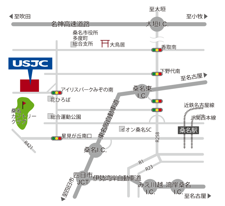
| Location | 2000, Mizono, Tado-cho, Kuwana, Mie, 511-0118, Japan |
|---|---|
| Plant Manager | Nobuhiro Misawa |
| Completion | April,2005 (300㎜ Plant) |
| Products | 300㎜ Logic Semiconductor Wafer |
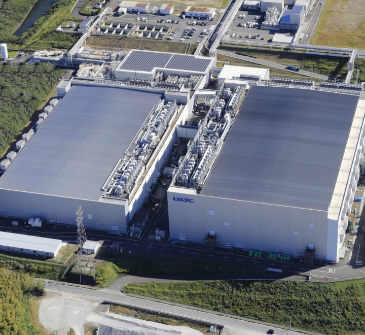
Mie 300㎜
Production Line
Plant Manager's Message
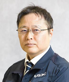
Nobuhiro Misawa,
Mie Plant Manager
The Mie Plant started operation as core plant for advanced semiconductor divices in October 1984.
With the understanding and support of people in the local community, we provide high-quality technology and services to customers around the world using sophisticated manufacturing techniques and our proprietary technology.
We will continue to strive to be a factory that is loved and trusted by all stakeholders.
Features
-

Since 1984, when we started operation as a base for development, prototyping, and mass production of logics, bipolar transistors, and memory, Mie Plant has contributed to the growth of the entire Japanese semiconductor industry for 40 years.
Corporate History -
With the aim of becoming an environmentally friendly semiconductor manufacturing fab, we make efforts such as introducing the latest energy-saving technologies and effectively using resources.
Plant Safety & Security Initiative -

We take advanced disaster risk measures, such as being the first in the world to introduce hybrid earthquake-proof buildings, ensuring a backup power supply using Li capacitors, and deploying LNG satellite bases.
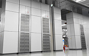
Mie 300㎜ Production Line
Mie 300㎜ Production Line
From the beginning of operations, Mie Plant has been mainly providing foundry services for the advanced logic LSIs, and has established manufacturing, information management, quality control, and customer support systems for the foundry business In accordance with ISO14001. We pursue “Green Fab”. According to the ISO9000 series and automotive IATF16949 certifications, we have established quality assurance and control systems. Additionally, we have been making our utmost efforts towards safety and quality improvements.
| Fab B1 | Fab B2 | |
|---|---|---|
| Start of operations |
2005 | 2007 |
| Total floor area |
38,000㎡ | 80,000㎡ |
| Clean room area |
17,000㎡ | 30,000㎡ |
| Location | Kuwana City, Mie Prefecture | |
| Wafer size | 300㎜ | |
| Process technology |
40㎚・55㎚・65㎚・90㎚ | |
| Production capacity |
About 39,800 wafers/month | |
| International Certifications |
ISO9001・ISO14001・IATF16949・ISO27001・ISO22301・ISO45001・IECQ QC 080000 | |
| Major features |
We deal with the risk of large-scale disasters by having clean rooms with earthquake-proof construction, a liquefied natural gas satellite base, and LIC (Lithium-ion capacitor). | |
Disaster Management
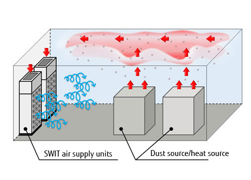
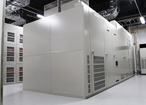
SWIT®(Swirling Induction Type HVAC System)®
The cleanroom uses SWIT, or swirling induction type HVAC, which creates temperature strata inside the cleanroom, and works with rising air currents created by heat-generating equipment to carry airborne dust toward the ceiling. This makes it possible to maintain a steady temperature in the work areas at lower elevations in the room more efficiently, so that the volume of air being supplied can be lower than in conventional HVAC systems. Also, because this allows for air to be supplied at a higher temperature, the chilled-water temperature can also be higher, which contributes to energy savings. Compared to existing systems, the annual energy used is expected to be roughly 47% lower for transport power and roughly 32% lower for heat-source power (*1).
Earthquake-proof Construction
For our earthquake management, we are the first semiconductor fab in the world to adopt a hybrid seismic isolation structure. Three types of seismic isolation systems have been placed between the building and its foundation, which under normal conditions minimize the effect of fine vibrations, allowing us to achieve a stable supply for our customers.
-
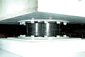
Seismic Isolation System: “Laminated rubber supports” A rubber bearing that absorbs vibrations and attenuates the swaying of the building.
-
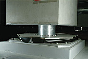
Seismic Isolation System: “Solid sliding supports” A Teflon-coated sliding face that slides horizontally and absorbs the building's vibrations.
-
Seismic Isolation System: “Oil damper” This restricts the range of lateral movement of the Solid sliding supports bearing.
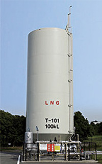
LNG Base
In preparation for a stoppage of the supply of city gas in the event of a large scale disaster, we have installed a liquefied natural gas (LNG) satellite base. As a result, in the event of a stoppage of gas, we are able to supply LNG using the satellite base and tanker vehicles. We continue to further strengthen our fab infrastructure against such disasters.
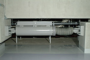
Lithium-ion Capacitor
As a countermeasure against instantaneous voltage drops or power failures, we have adopted LIC (Lithium-ion Capacitor). This enables the continuous operation of a stable fab.
Lithium-ion Capacitor (LIC)