How a semiconductor wafer is made
Manufacturing a semiconductor IC requires as many as hundreds of microfabrication steps.
This section provides an overview of the process flow of wafer processing.
Supplementary information
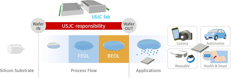
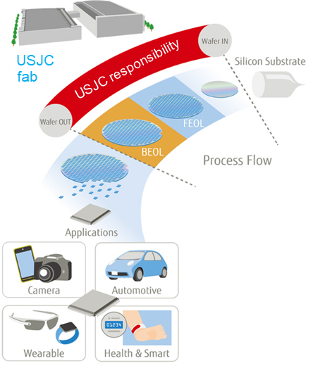
Process Flow
USJC undertakes wafer processing as a foundry company to manufacture semiconductor ICs. This section provides an overview of the process flow of wafer processing.
FEOL (Front End of Line: substrate process, the first half of wafer processing)
Components such as transistors are formed on a silicon substrate.
- 1Isolation
-
Isolation
-
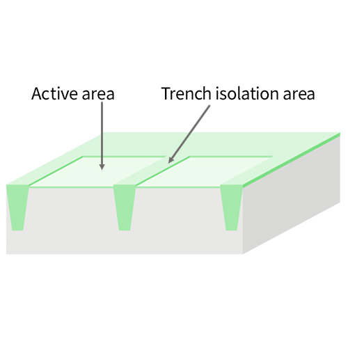
Transistors are formed near the silicon wafer surface.
To ensure that each transistor operates independently, it is necessary to prevent interference with other neighboring transistors. Therefore, the regions where transistors are to be formed are isolated. There are a number of methods for this isolation.
The technique introduced here is called STI (Shallow Trench Isolation). -
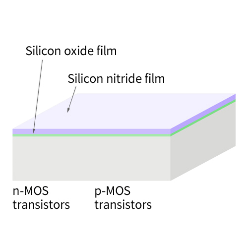
1. Oxide + nitride film growth
First a silicon oxide film is formed by oxidizing a silicon wafer, and then a silicon nitride film is formed using the CVD method.
-
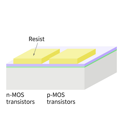
2. Resist pattern formation
A resist pattern is formed.
-
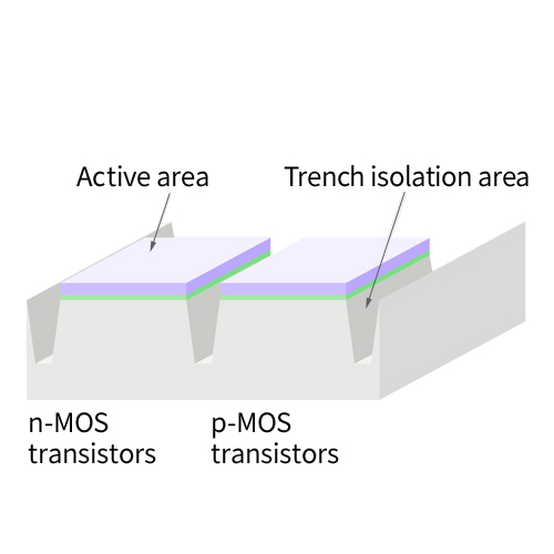
3. Shallow trench formation
Using the resist pattern as a mask, shallow trenches are cut by etching the silicon nitride film, silicon oxide film and silicon wafer.
-
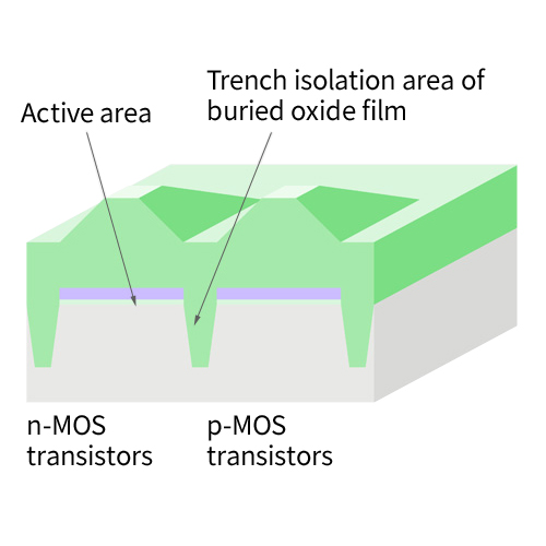
4. Buried oxide film growth
Trenches are filled by forming a thick silicon oxide film using the CVD method.
-
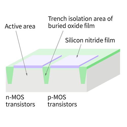
5. Buried oxide film polishing
The surface is polished to remove the excess silicon oxide film, and the silicon oxide film is left only in the trenches.
-
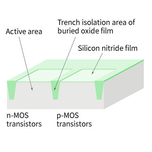
6. Nitride film removal
The silicon nitride film is removed using chemical treatment.
-
- 2Well and channel formation
-
Well and channel formation
-
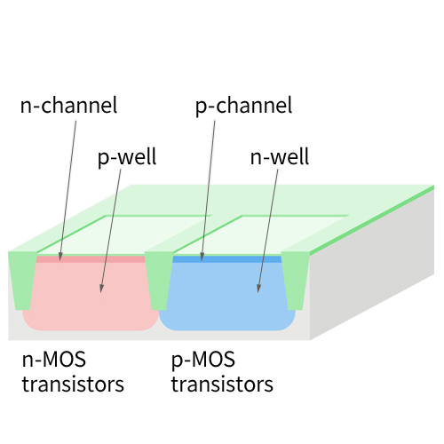
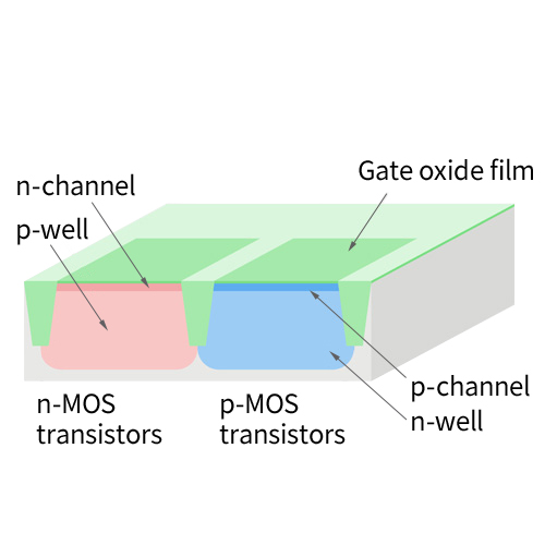
N-MOS transistors and p-MOS transistors are formed in a chip.
Impurities appropriate for n-MOS transistors and p-MOS transistors are respectively implanted into the Si surface at appropriate concentrations in the regions where the transistors are to be formed (n-MOS: p-well, n-channel; p-MOS: n-well, p-channel). In the case where transistors with two or more different voltages and characteristics are made, impurity implantation of different dopants/dosages is additionally performed.
Repeat “2-3. n-Channel” and “2-4. p-Channel. -
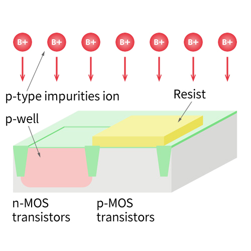
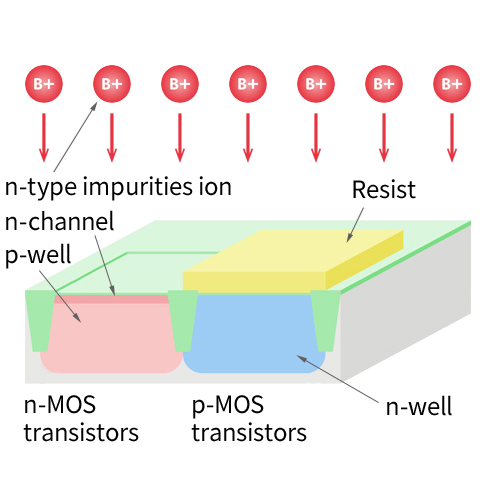
1. p-Well
A resist pattern is formed to cover the p-MOS area, and p-type impurities (e.g., boron (B)) are implanted in the n-MOS area.
After implantation, the resist pattern is removed. -
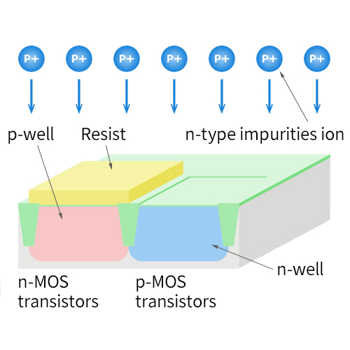
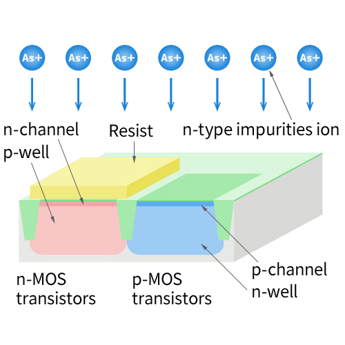
2. n-Well
A resist pattern is formed to cover the n-MOS area, and n-type impurities (e.g., phosphorus (P)) are implanted in the p-MOS area.
After implantation, the resist pattern is removed. -
3. n-Channel
A resist pattern is formed to cover the p-MOS area, and p-type impurities (e.g., boron (B)) are implanted in the n-MOS area.
After implantation, the resist pattern is removed. -
4. p-Channel
A resist pattern is formed to cover the n-MOS area, and n-type impurities (e.g., arsenic (As)) are implanted in the p-MOS area.
After implantation, the resist pattern is removed.
-
- 3Gate oxidation and gate formation
-
Gate oxidation and gate formation
-
This step is most important from the viewpoint of transistor characteristics.
A gate oxide film greatly influences the performance and reliability of a transistor, and should therefore be a high-density thin film uniformly distributed over the wafer surface.
Since the size of the gate formed may also greatly influence the performance of the transistor, strict dimensional control is necessary in both photo resist patterning and gate etching.
Gate electrodes are formed of polysilicon (polycrystalline silicon) by CVD. -
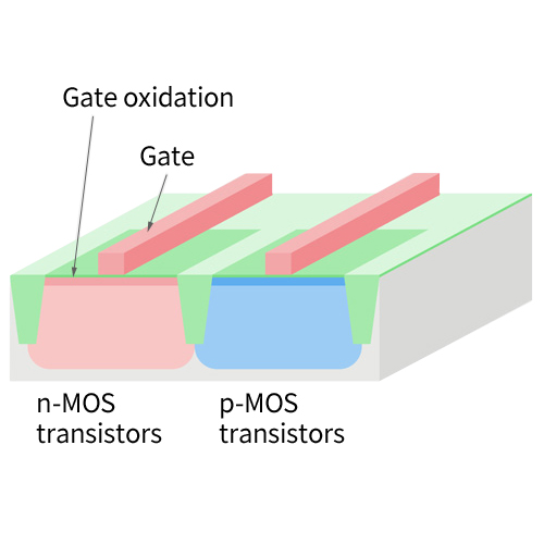
1. Gate oxidation
The silicon surface is cleaned through chemical treatment, and then oxidized, forming a gate oxide film. The thickness and quality of this oxide film has a major effect on transistor performance and reliability, and thus it must be a thin, high-density film with a uniform distribution.
-
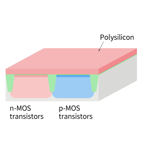
2. Polysilicon growth
Polysilicon (polycrystalline silicon) to be the gate electrode is formed using the CVD method.
-
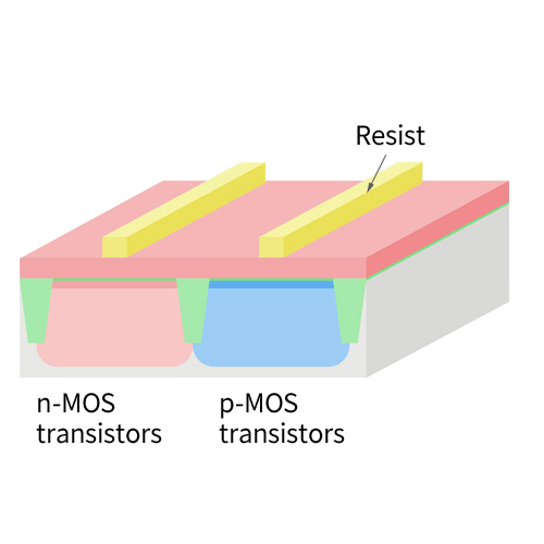
3. Formation of gate resist pattern
Gate resist pattern is formed.
-
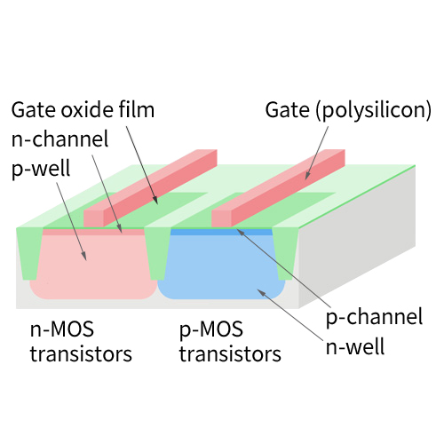
4. Gate etching
Using the gate resist pattern as a mask, the gate is formed by etching the polysilicon and gate oxide film. After etching, the resist pattern is removed. Gate dimensions have a major effect on transistor performance, and thus strict dimensional control is needed in both gate resist patterning and gate etching.
-
- 4LDD formation
-
LDD formation
-
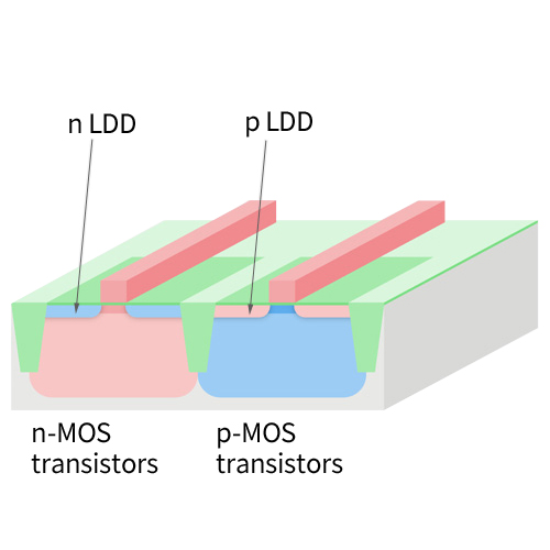
To avoid adverse effects (such as slower operation speed) of transistor miniaturization, LDDs (Lightly Doped Drains, low density impurity drains) are formed.
LDDs are also called extensions.
N-LDD: N-type impurities (e.g., As+, P+) are implanted into n-MOS areas.
P-LDD: P-type impurities (e.g., B+) are implanted into p-MOS areas. -
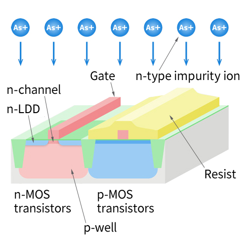
1. n-LDD
p-A resist pattern is formed to cover the p-MOS area, and n-type impurities (e.g., phosphorus (P), arsenic (As)) are implanted in the n-MOS area.
After implantation, the resist pattern is removed. -
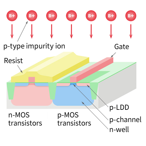
2. p-LDD
A resist pattern is formed to cover the n-MOS area, and p-type impurities (e.g., boron (B)) are implanted in the p-MOS area.
After implantation, the resist pattern is removed.
-
- 5Side wall spacers
-
Side wall spacers
-
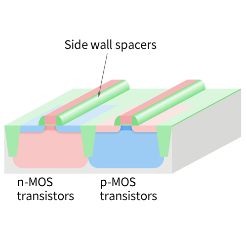
An oxide film is formed only at side wall portions of gates for LDD formation (above mentioned) and salicidation (described below) of gates, sources, and drains.
Side wall oxide film: A silicon oxide film is formed on the entire wafer surface. Side wall etching: Anisotropic etching (vertical direction) is performed on the oxide film so that the oxide film may be left only on gate side walls. -
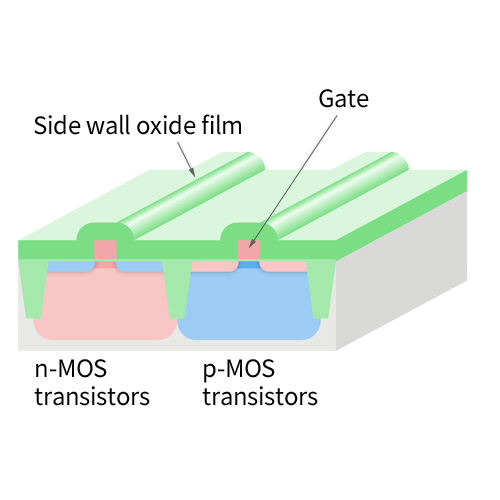
1. Side wall oxide film growth
A silicon oxide film is formed using the CVD method over the entire surface of the silicon wafer.
-
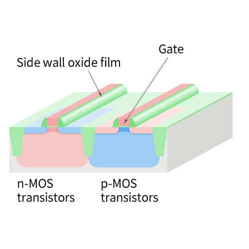
2. Side wall etching
If anisotropic etching is performed on the oxide film formed over the entire surface, it is possible to leave an oxide film only at the gate side walls. This sort of etching which does not use a resist pattern is called etching back.
-
- 6Source/drain
-
Source/drain
-
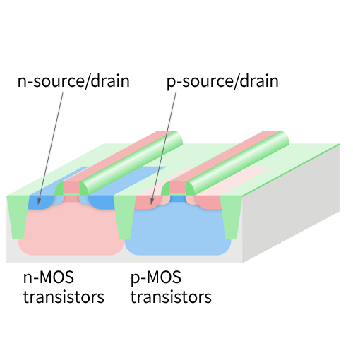
Sources and drains are formed in n-MOS areas and p-MOS areas. The shapes of sources and drains are the same because usual transistors are symmetric. Which is a source or a drain is defined depending on the connection direction of the power supply.
P-source/drain: P-type impurities (e.g., B+) are implanted into p-MOS areas.
N-source/drain: N-type impurities (e.g., As+, P+) are implanted into n-MOS areas. -
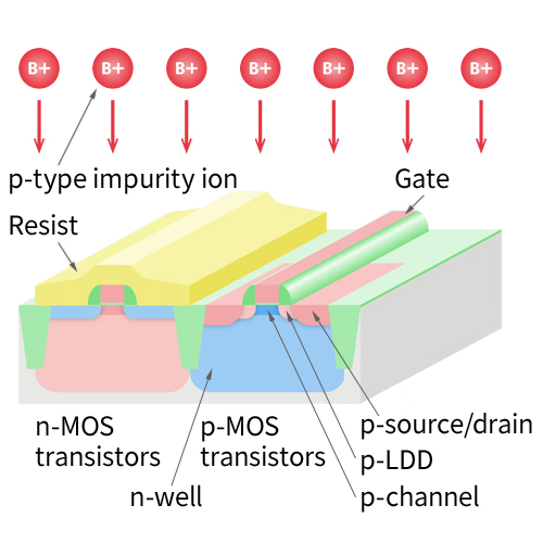
1. p-Source/drain
A resist pattern is formed to cover the n-MOS area, and p-type impurities (e.g., boron (B)) are implanted in the p-MOS area.
After implantation, the resist pattern is removed. -
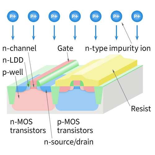
2. n-Source/drain
A resist pattern is formed to cover the p-MOS area, and n-type impurities (e.g., phosphorus (P), arsenic (As)) are implanted in the n-MOS area.
After implantation, the resist pattern is removed.
-
- 7Silicide
-
Silicide
-
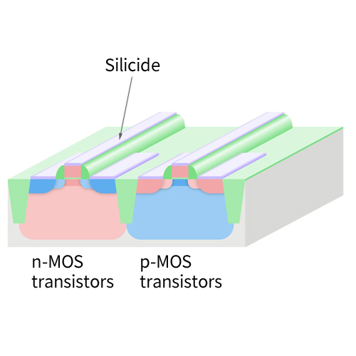
Silicide (compound of silicon with metal) is formed on gates (polysilicon), sources and drains (Si wafer) as three MOS transistor electrodes in order to reduce contact resistance to metal wiring layers to be formed later. This silicide formation also has the effect of lowering the resistance of each electrode.
Salicidation: A cobalt film is removed selectively by chemical etching (Self aligned silicide). -
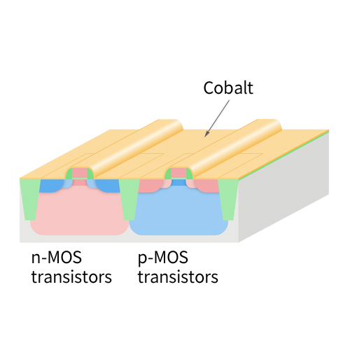
1. Cobalt film deposition (sputtering)
A cobalt film is formed on the silicon wafer surface using the PVD method (sputtering). Metals other than cobalt used for silicide include nickel and titanium.
-
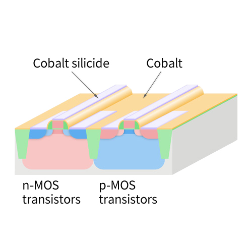
2. Cobalt silicide formation
If a silicon wafer whose surface is coated with a cobalt film is heated, the part where the silicon and cobalt are in contact changes to cobalt silicide. Cobalt on the oxide film remains as cobalt.
-
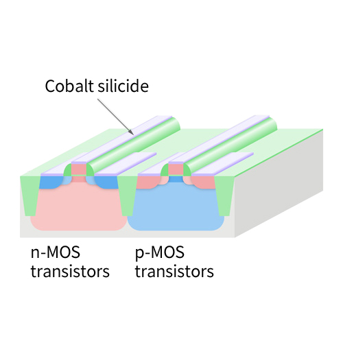
3. Cobalt removal
A cobalt film is removed selectively by chemical etching. Silicide remains on the gate, source and drain. Formation of silicide through self-alignment in this way is called salicide (self aligned silicide).
-
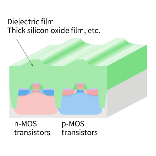
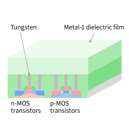
- 8Dielectric film
-
Dielectric film
-
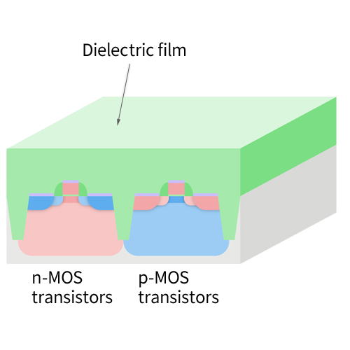
The interconnect process for connecting elements such as transistors starts from this step.
Dielectric film deposition: A thick silicon oxide film or the like is formed by CVD.
Dielectric film polishing: The silicon oxide film is polished for the film planarization of the wafer surface. -
1. Dielectric film formation
A thick film of silicon oxide or similar material is formed on the silicon wafer surface using the CVD method.
-
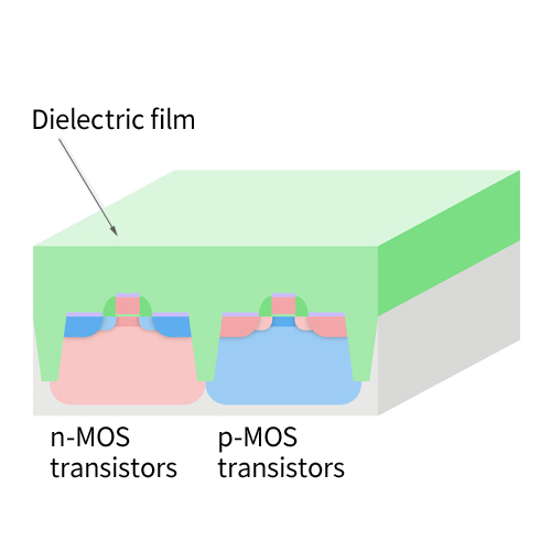
2. Polishing of dielectric film
Simply forming a dielectric film results in unevenness of the wafer surface and interferes with subsequent processing.
The oxide film on the surface is polished to make it smooth.
-
- 9Contact holes
-
Contact holes
-
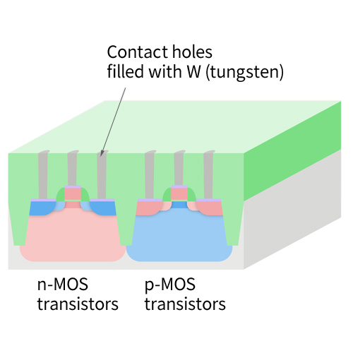
To connect electrodes such as gates, sources, and drains of transistors to metal wiring layers, contact holes are made in the dielectric film and filled with W (tungsten).
Plug-tungsten filling: Tungsten is deposited in contact holes.
Plug-tungsten polishing: The surface is polished to remove excess tungsten and leave tungsten only in the contact holes. -
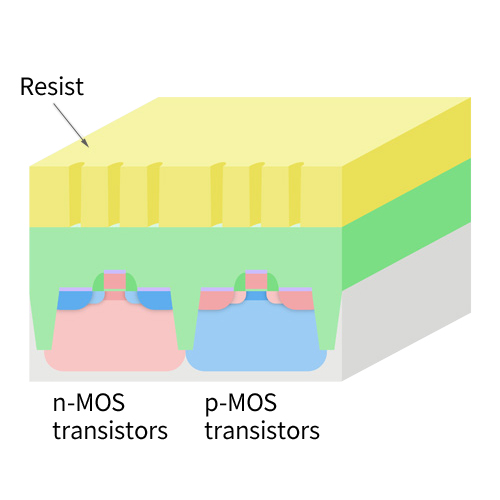
1. Formation of contact hole resist pattern
A resist pattern for contact holes is formed.
-
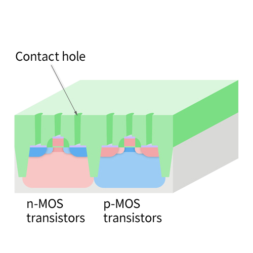
2. Contact hole etching
Using the contact hole resist pattern as a mask, contact holes are formed in the dielectric film by performing etching treatment. After etching, the resist pattern is removed. These holes are extremely small and deep (high aspect ratio), and thus great care must be taken to control hole diameter and depth.
-
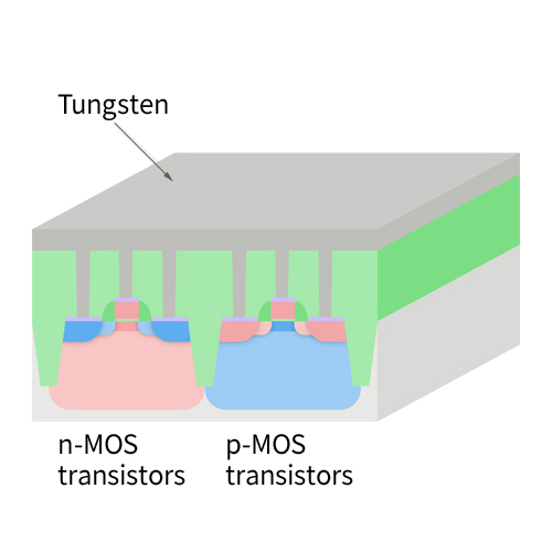
3. Plug-tungsten filling
A tungsten film is formed on the silicon wafer surface using the CVD method, and the contact holes are filled.
-
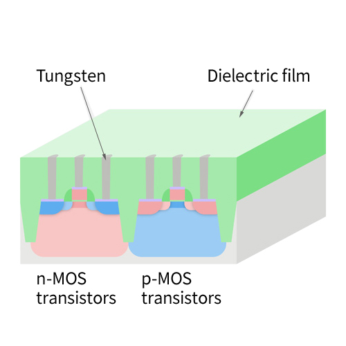
4. Plug-tungsten polishing
The surface is polished and excess tungsten film is removed. Tungsten is left only in the contact holes.
-
BEOL (Back End of Line: interconnect process, the second half of wafer processing)
Components formed in the FEOL are interconnected with metal material to form circuits.
- 10Metal-1
-
Metal-1
-
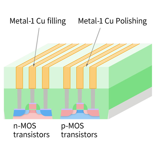
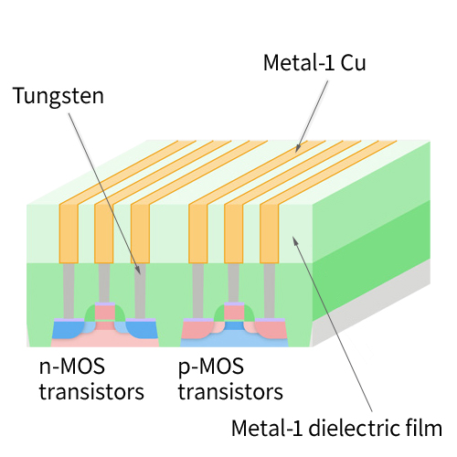
A dielectric film is deposited as an inter layer dielectric, a trench pattern is formed by photo resist patterning and etching, and trenches are filled with Cu (copper) metal by electroplating.
The method of filling only the trenches with Cu is called single damascene.
Metal-1 Cu filling: A Cu film is deposited in the trenches by electroplating.
Metal-1 Cu Polishing: Excess Cu is removed by surface polishing to leave Cu only in the trenches. -
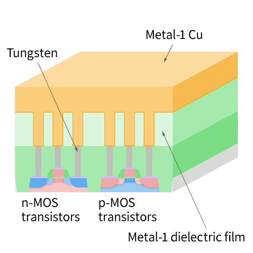
1. Growth of metal-1 dielectric film
A thick film of silicon oxide or similar material is formed on the silicon wafer surface using the CVD method.
-
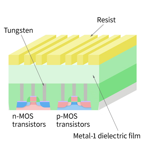
2. Formation of metal-1 trench resist pattern
A resist pattern for the metal-1 trench is formed.
-
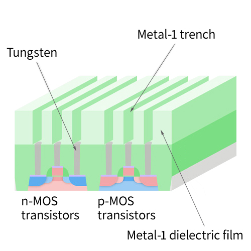
3. Metal-1 trench etching
Using the metal-1 trench resist pattern as a mask, trenches are formed in the dielectric film by performing etching treatment. After etching, the resist pattern is removed.
-
4. Metal-1 Cu burial
A Cu film is formed through electroplating, and the trenches are filled.
-
5. Metal-1 Cu polishing
Excess Cu film is removed by polishing the surface, and Cu is left only in trenches.
-
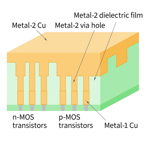
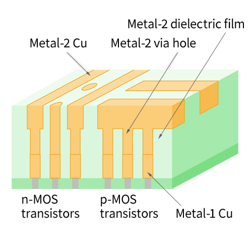
- 11Metal-2
-
Metal-2
-
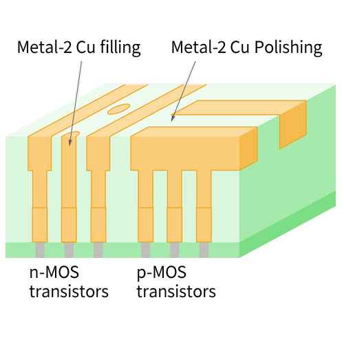
A dielectric film is deposited as an inter metal dielectric, a trench and via pattern is formed by photo resist patterning and etching, and trenches and vias are filled with Cu (copper) metal by electroplating. The method of filling trenches and vias with Cu at the same time is called dual damascene.
Metal-2 Cu filling: A Cu film is deposited in the trenches and the vias by electroplating.
Metal-2 Cu Polishing: Excess Cu is removed by surface polishing to leave Cu only in the trenches and the vias.
In accordance with the circuit scale, wiring is layered by repeating the steps from “11-1. Growth of metal-2 dielectric film” to “11-6. Metal-1 Cu polishing.” -
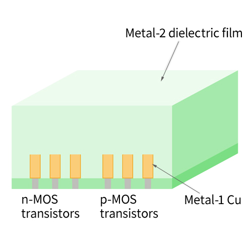
1. Growth of metal-2 dielectric film
A thick film of silicon oxide or similar material is formed on the silicon wafer surface using the CVD method.
-
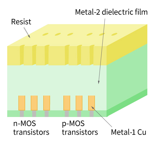
2. Formation of metal-2 via hole resist pattern
A resist pattern for via hole is formed.
-
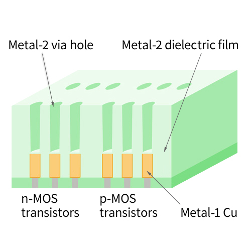
3. Metal-2 via hole etching
Using the via hole pattern as a mask, via holes are formed in the dielectric film using etching treatment. After etching, the resist pattern is removed.
-
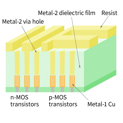
4. Formation of metal-2 trench resist pattern
A resist pattern is formed for metal-2 trenches.
-
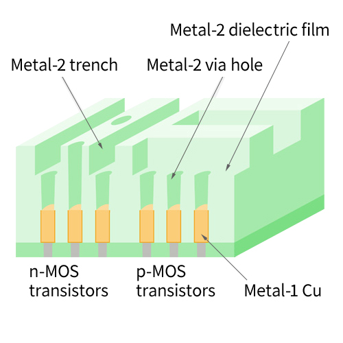
5. Metal-2 trench etching
Using the metal-2 trench pattern as a mask, trenches are formed in the dielectric film by performing etching treatment. After etching, the resist pattern is removed.
-
6. Metal-2 Cu burial
A Cu film is formed using electroplating, and the via holes and trenches are filled.
-
7. Metal-2 Cu polishing
Excess Cu film is removed by polishing the surface, and Cu is left only in via holes and trenches.
-